


Design Bias Tees
 This article describes the design of bias tees for a pulsed-bias, pulsed-RF test system. The cut-off frequency of the DC path was raised to allow pulsing of the bias signal. The theory of bias tee design for pulsed measurements is first presented. The simulation results for the design without the use of component models are presented, followed by simulation results obtained using accurate parasitic models for the inductor and capacitor used. The simulation results are then compared with S-parameter measurements obtained using a TRL calibration and found to show good agreement. Finally, illustrations of the accurate use of the bias-tee in performing both pulsed IV and pulsed S-parameter measurements are provided.
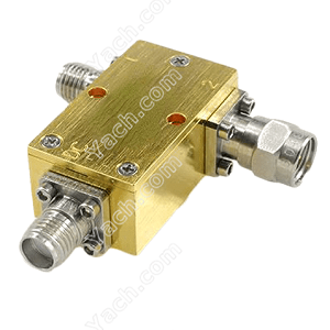
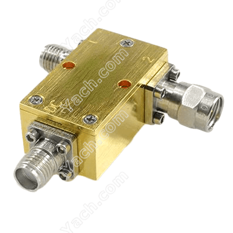
The typical bias tees circuit consists of an inductor and a capacitor, as shown in Figure 1. The function of a bias-t is to simultaneously allow a DC bias voltage and an RF test signal to be applied to the port of a transistor during measurement. Such as in an S-parameter measurement system, the DC bias-t is applied at the port labeled Ą°DC,Ąą and the RF test signal from the vector network analyzer is applied to the port labeled Ą°RF.Ąą At the RF + DC port, both the RF and DC voltages are applied to the device. The purpose of the inductor is to prevent the RF signal from entering the DC path, and the purpose of the capacitor is to keep the DC signal from entering the RF path. The inductor and capacitor should be designed such that the upper cut-off frequency of the low pass DC path is lower than the lower cut-off frequency of the high pass RF path.
Where R is the total resistance seen at the capacitor terminals. In this case, the termination at the RF port is 50 Ķļ and the termination at the RF + DC port is large (either the input or output impedance of the device) in normal operation but will be 50 Ķļ in the bias tee test setup. In operation, however, the value of the input resistance will be fairly large, changing the cut-off frequency. However, in a 50 Ķļ test system, 50 Ķļ is the impedance at all test ports. This setup will be used for the purpose of benchmarking the behavior of the device through measurement and simulation. Thus, R = 50 + 50 = 100 Ķļ for this case.
In this case, R is equal to the sum of the impedance presented by the bias-t and the input impedance to the device under test. For a 50 Ķļ test system, R = 50 + 50 = 100 Ķļ.
The outstanding factor for a pulsed bias tees design is that the cut-off frequency of the DC path must be high enough to allow the pulsed bias signal to proceed unabated from the DC to the RF + DC ports. In this case, the smallest pulse length to be used for pulsing the bias-t is approximately 100 ns. The frequency content of this pulse is a (sin x)/x function centered at a frequency of 1/(100 ĄÁ 10ĻC9) = 10 MHz. Thus, the upper cut-off frequency of the bias network should be greater than 10 MHz, large enough that the entire frequency content of the pulse can pass through the DC path without distortion, this will allow the integrity of the pulse shape to be maintained.
- ÉÏŌŧÆŠĢšTesting performance [2022-05-04]
- ÏÂŌŧÆŠĢšWork principle of bias-t [2022-05-04]